PCB Design With KiCad: The Electronics Secret Revealed! How to get your kicad pcb design ready for fabrication
If you are looking for Kicad Electronic Circuit Design Part 2 Pcbnew Pcb Des - vrogue.co you've came to the right page. We have 25 Images about Kicad Electronic Circuit Design Part 2 Pcbnew Pcb Des - vrogue.co like PCB Design in PcbNew | KiCad EDA, KiCad PCB Layout Quick Tips - Embedded Computing Design and also How To Make Pcb With Kicad Pcb Designs - Vrogue. Here you go:
Kicad Electronic Circuit Design Part 2 Pcbnew Pcb Des - Vrogue.co
 www.vrogue.co
KiCad Version 6.0.0 With New Interface And Improved PCB Design
 www.electronics-lab.com
KiCAD PCB Design Course - Learn To Design You Own Circuit Boards
 deepbluembedded.com
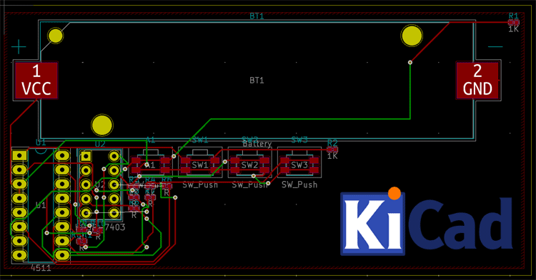
kicad pcb library
Gallery Led Vu Meter Pcb Design Using Kicad Hackaday - Vrogue.co
 www.vrogue.co
How To Get Your KiCad PCB Design Ready For Fabrication - CIRCUITSTATE
 www.pinterest.com
KiCad PCB Layout Quick Tips - Embedded Computing Design
 pcb-design.pages.dev
KiCad EDA Schematic Capture PCB Design Software, 55% OFF
 www.gbu-presnenskij.ru
PCB Design/Kicad | Tufts ME 30
 andnowforelectronics.com
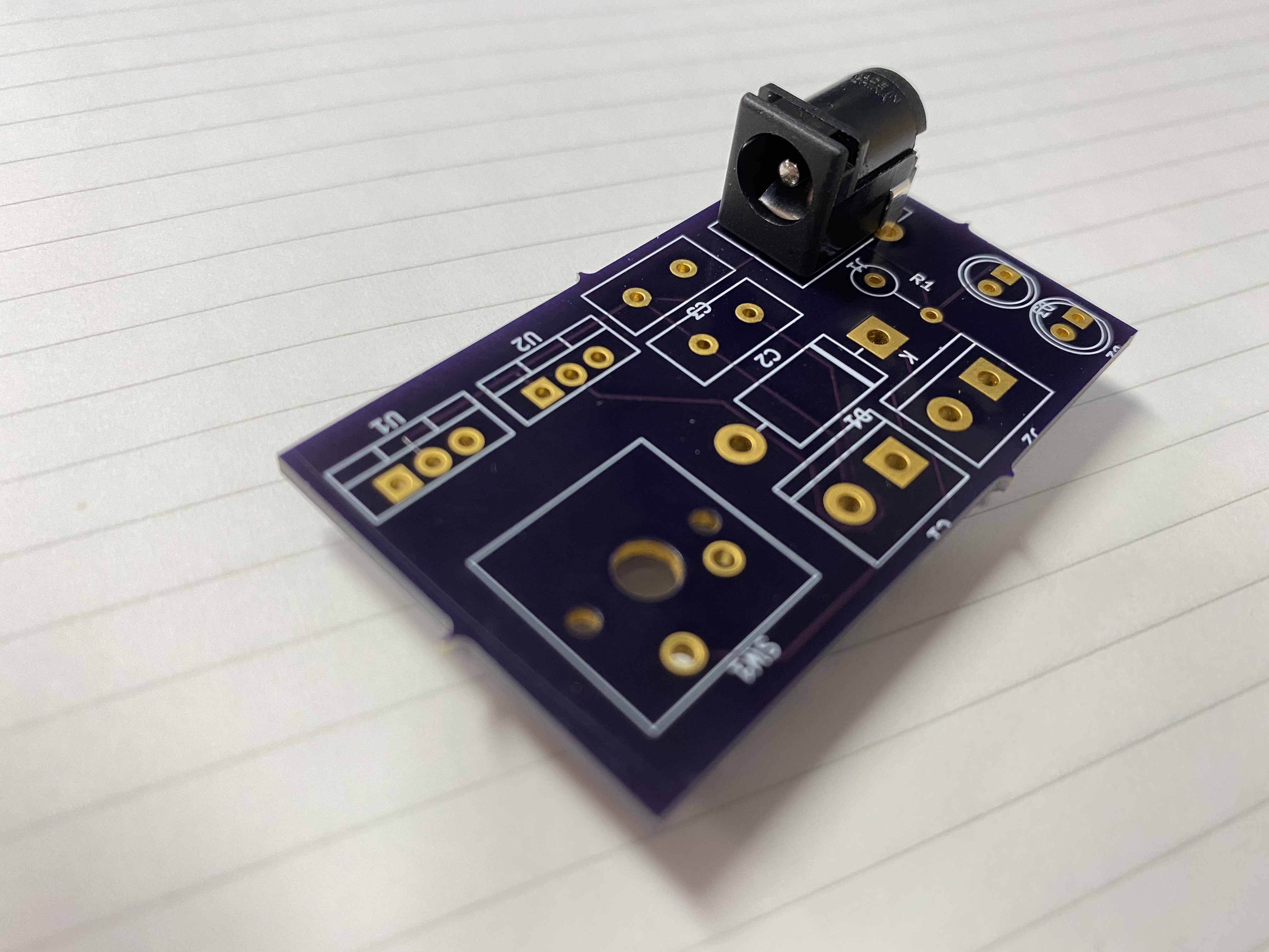
pcb jack
Pcb Design Kicad Tutorial 4 Layer Pcb Design Tutorial Kicad Pcb Designs
 pcbways.pages.dev
KiCad (32-bit) Download (2023 Latest)
 www.filehorse.com
How To Make Pcb With Kicad Pcb Designs - Vrogue
 www.vrogue.co
Introduction To PCB Design Using KiCad | The Hardware Academy
 thehardwareacademy.com
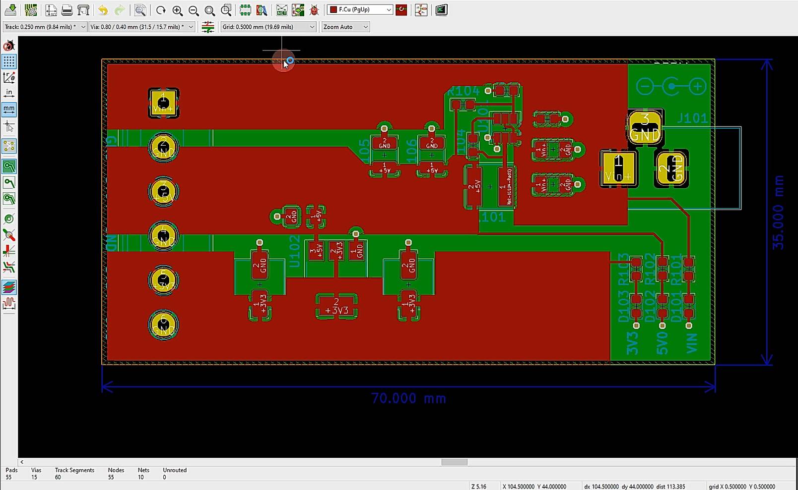
pcb kicad
Fillable Online Kicad Eda Schematic Capture Pcb Design - Vro
 www.vrogue.co
Kicad Pcb Layout Pcb Designs | Images And Photos Finder
 www.aiophotoz.com
Flex Pcb Design Kicad Kicad Flex Generating Rigid Method Work Info Kb
 pcbways.pages.dev
4 Layer Pcb Design Tutorial Kicad Pcb Designs | Hot Sex Picture
 www.hotzxgirl.com
How To Get Your KiCad PCB Design Ready For Automated Assembly – KiCad 6
 circuitstate.com
How To Make Pcb With Kicad Pcb Designs - Vrogue
 www.vrogue.co
Kicad Electronic Circuit Design Part 2 Pcbnew Pcb Des - Vrogue.co
 www.vrogue.co
Kicad Electrical Wiring Diagram - Wiring Work
 www.wiringwork.com
PCB Design In PcbNew | KiCad EDA
 kicad.io
Resuelto Arduino Nano Kicad Simbolos Arduino Uno Pcb Design
 www.vrogue.co
Pcb Designing Kicad Tutorial Introduction Part 1 Elec Vrogue
 www.vrogue.co
Pcb Design - KiCad PCB: Enlarging Areas - Electrical Engineering Stack
 electronics.stackexchange.com
Workaround Pcb Step Export Into Solidworks D Models Kicad Info Forums
 www.hotzxgirl.com
Resuelto arduino nano kicad simbolos arduino uno pcb design. Fillable online kicad eda schematic capture pcb design. Introduction to pcb design using kicad